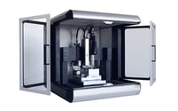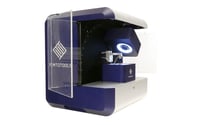

The NMT04 is specially designed to work seamlessly with Electron Backscatter Diffraction (EBSD) or Scanning Transmission Electron Microscopy (STEM) detectors inside the SEM. Its open measurement frame enables clear view of the sample during deformation, allowing simultaneous observation and analysis of the evolution of the microstructure of the sample during mechanical testing. This allows the study of stress-strain response of materials, not only in correlation with surface event observation in the SEM, but also with EBSD, TKD, and STEM characterization to gain unprecedented quantitative insights into phase transformation and dislocation dynamics.
By applying a pattern to the surface of the sample, the stresses in the material can be monitored by Digital Image Correlation (DIC) during the mechanical analysis. Moreover, in-situ EBSD measurements during micro-tension, pillar compression, or cantilever bending enable the monitoring and quantification of dynamic phase transformations and strain localization during deformation. To visualize plasticity at the dislocation scale, micro-tensile testing of electron-transparent specimens and thin films can be performed while conducting TKD and STEM analyses.
Application Examples
- 01 In-Situ Tensile Test
- 02 Simultaneous DIC
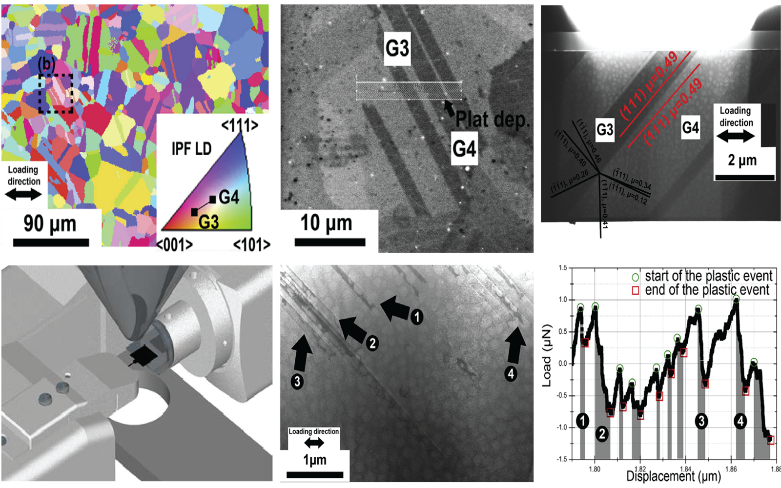
Simoultaneus Mechanical Testing with STEM and EBSD
In-situ tests of nickel-based superalloy oligocrystals in a scanning electron microscope revealed dislocation dynamics during tensile loading.
After selecting a proper location, in terms of microstructure and crystal orientation using SEM and EBSD, a specimen was extracted by focused-ion beam (FIB) machining, placed on a testing sample support (e.g. FemtoTool’s Nano-Tensile testing chip), and secured using Ion (or electron) beam induced deposition. FIB carving and thinning of the micro-tensile specimen down to electron transparency was then performed with low voltage to minimize FIB damage and enable STEM imaging.
Dislocation behavior near twin boundaries, precipitate shearing, and antiphase boundary-coupled shearing within slip bands was successfully revealed. These findings offer new insights into strain localization, plastic localization, and fatigue crack initiation near twin boundaries in superalloys.
Micro-Shear of Silicon as Observed by Digital Image Correlation (DIC)
In this example, acquired in collaboration with the Laboratory for Nanometallurgy at ETH Zurich, [110]-oriented Silicon is sheared directly on its primary slip planes at 600 °C. Color strain maps are provided using digital image correlation (DIC) using the speckle patterns and in-situ imaging at temperature in the SEM. This enables direct measurement of the local strains within the shear zones.
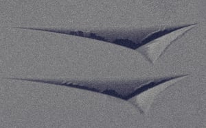
Nanoindentation
READ MORE ->
Read More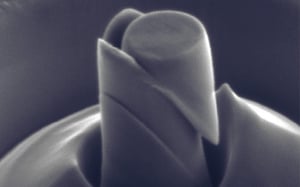
Micro-Pillar Compression
READ MORE ->
Read More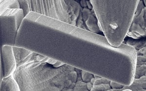
Micro-Cantilever Testing
READ MORE ->
Read More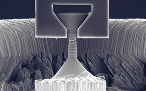
Micro-Tensile Testing
READ MORE ->
Read More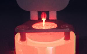
High-Temperature Testing
READ MORE ->
Read More
Mechanical Microscopy
READ MORE ->
Read More
Correlative Mechanical Microscopy
READ MORE ->
Read More
Scratch Testing
READ MORE ->
Read More
